

ADDRESS:
CTLAB
Central European Institute of Technology
Purkynova 123, 612 00 Brno
Czech Republic
+420 541 142 875
VAT: CZ00216305


New expertise for electronic devices
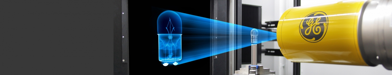
Our portfolio of non-destructive testing expertizes has newly expanded by digital radiography (X-ray imaging). This extension is a result of a long-term cooperation with PBT Rožnov p.R., s.r.o., within which we can use professional inspection system GE phoenix microme|x (https://www.industrial.ai/phoenix-micromex) in a shared laboratory regime.
Microme|x is designed especially for inspection of complicated DPS and SMT assemblies. High resolution is achieved thanks to the open X-ray tube. Inner arrangement guarantees unbeatable magnification allowing to inspect soldered printed circuit boards or even microcracks in the balls of BGA. Maximal available voltage 180 kV enables to inspect also challenging assemblies with coolers or metal cases mounted.
X-ray images are post-processed by unique software tools for local contrast enhancement in order to reveal material defects. The software also allows to quantify porosity in the soldered joints. Inspection of bigger amount of identical samples can be partially automated for NOK/OK samples sorting. Last but not least, microme|x can use advanced methods such as planar CT (laminography), enabling to visualize multilayer structures in 2D cross-sections.
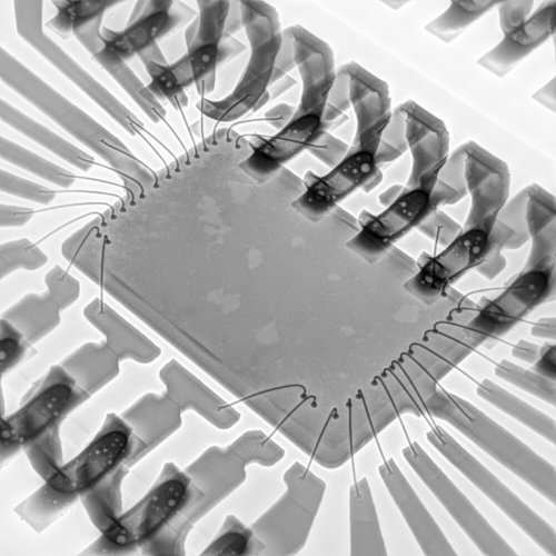
Filtered X-ray image of a microchip soldered to PCB.